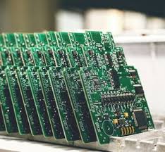
Enhanced Functionality and Compact Size
Multi-layer PCBs (Printed Circuit Boards) are pivotal in today’s advanced electronics. By stacking multiple layers of circuitry, these boards provide a significant leap in functionality compared to their single-layer counterparts. One of the most prominent benefits is the increased area available for wiring. This is crucial for complex circuits used in smartphones, computers, and medical devices, where space is at a premium.
In practice, a multi-layer PCB can offer as much as a tenfold increase in area for circuitry compared to a single-layer PCB, within the same footprint. For example, a standard smartphone might use a 10-layer PCB to accommodate all the necessary components and connections within a slim design.
Improved Signal Integrity
Signal integrity is critical in high-speed electronic devices, and multi-layer PCBs excel in maintaining robust signal quality. By designing specific layers as ground and power planes, these boards reduce electromagnetic interference (EMI) and enhance signal integrity. The result is faster transmission speeds and reduced signal loss, crucial for devices like routers and gaming consoles.
Research shows that multi-layer PCBs can reduce EMI by up to 20% compared to double-layer PCBs. This is particularly vital in environments where electronic devices must operate without interference from other electronic devices or external sources.
Enhanced Durability and Reliability
Multi-layer PCBs are designed to withstand harsh conditions, making them ideal for use in automotive and aerospace industries. The manufacturing process involves high-temperature lamination which bonds the layers together under pressure, creating a single, durable unit. This process enhances the board's mechanical strength, allowing it to endure vibrations and shocks better than single-layer PCBs.
Field data indicate that multi-layer PCBs have a failure rate that is approximately 30% lower than that of their single-layer counterparts over a typical 10-year life cycle in automotive applications. This reliability is critical for safety and performance in demanding applications.
Better Thermal Management
With the inclusion of middle layers that can act as additional heat dissipating surfaces, multi-layer PCBs manage heat more efficiently. This is essential for high-performance electronics where overheating can reduce efficiency and lifespan. Effective thermal management helps in maintaining optimal performance and extends the device's operational life.
Studies have demonstrated that multi-layer PCBs can improve heat dissipation by approximately 10-15% compared to two-layer boards in densely packed electronic assemblies, such as in LED lighting systems or high-performance computing hardware.
Cost Efficiency in the Long Run
While the upfront cost of designing and manufacturing multi-layer PCBs might be higher, the long-term savings are significant. Reduced failure rates, lower maintenance costs, and the longevity of the boards make them a cost-effective choice for industries where reliability and durability are paramount.
An analysis of lifecycle costs in the consumer electronics sector shows that using multi-layer PCBs can reduce the total cost of ownership by up to 25% over five years, factoring in reduced warranty claims and service needs.
Integrating a higher number of pcb layers not only maximizes the performance and reliability of electronic devices but also supports the development of more compact and robust products. As technology progresses, the role of multi-layer PCBs is becoming increasingly crucial in enabling the next generation of electronic innovation.